TLC2543
技术资料——
TLC2543 PDF技术资料
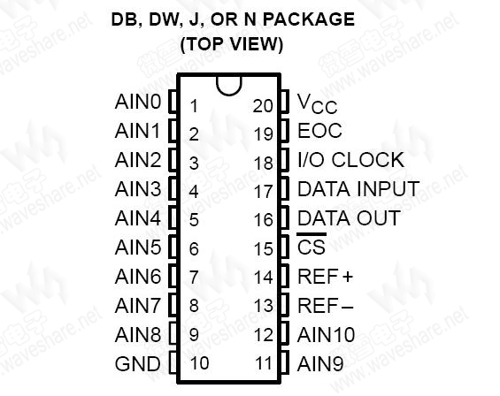
TLC2543 概述The TLC2543 are 12-bit, switched-capacitor, successive-approximation, analog-to-digital converters. Each TLC2543, with three control inputs [chip select (CS\), the input-output clock, and the address input (DATA INPUT)], is designed for communication with the serial port of a host processor or peripheral through a serial 3-state output. The device allows high-speed data transfers from the host. The TLC2543C is characterized for operation from TA = 0°C to 70°C. The TLC2543I is characterized for operation from TA = –40°C to 85°C. The TLC2543M is characterized for operation from TA = –55°C to 125°C. |
|
||||||||||||||||||||||||||||
|---|---|---|---|---|---|---|---|---|---|---|---|---|---|---|---|---|---|---|---|---|---|---|---|---|---|---|---|---|---|
TLC2543 特性
|
|||||||||||||||||||||||||||||