P89LPC932A1
技术资料——
P89LPC932A1 PDF技术资料
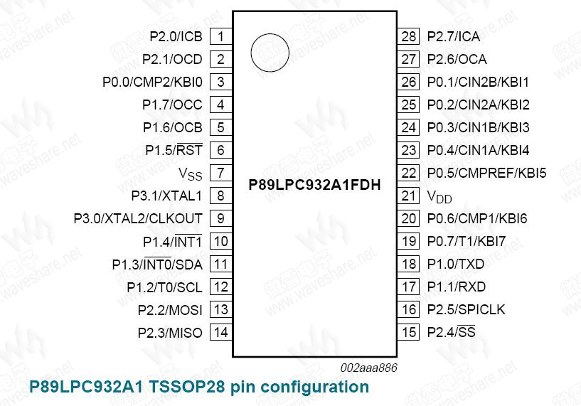
P89LPC932A1 概述P89LPC932A1是一款低成本单片封装微控制器。P89LPC932A1基于高性能的处理架构,执行指令仅需2到4个时钟周期,速度是标准80C51器件的6倍。P89LPC932A1集成了多种系统级功能,以便极大减少元件数目和减小电路板面积,从而降低系统成本。 |
|
||||||||||||||||||||||||||||||||||||||||||||||||||||
|---|---|---|---|---|---|---|---|---|---|---|---|---|---|---|---|---|---|---|---|---|---|---|---|---|---|---|---|---|---|---|---|---|---|---|---|---|---|---|---|---|---|---|---|---|---|---|---|---|---|---|---|---|---|
P89LPC932A1 特性
|
|||||||||||||||||||||||||||||||||||||||||||||||||||||