LPC1788
技术资料——
LPC1788 PDF技术资料
| LPC1788 存储器 | |
|---|---|
| Flash (KB) | 512 |
| RAM (kB) | 96 |
| EEPROM (kB) | 4 |
| LPC1788 其他参数 | |
| fmax (MHz) | 120 |
| I/O pins | 165 |
| UART | 5 |
| I²C | 3 |
| I²S | 1 |
| SSP/SPI | 3 |
| ADC (12-bit) | 8 |
| DAC (10-bit) | 1 |
| 定时器 | 4 |
| PWM | 6 |
| I/O 电压 (V) | 3.3 |
| CPU 电压 (V) | - |
| LPC1788 封装与引脚 | |
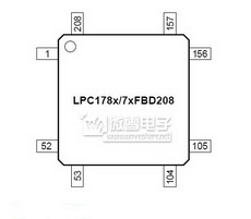
| LQFP208 | |
LPC1788 概述
The LPC1788 is a Cortex-M3 microcontroller for embedded applications featuring a high level of integration and low power consumption at frequencies of 120 MHz.
The LPC1788 features include 512 kB of flash memory, 96 kB of data memory, Ethernet, USB 2.0 Host/OTG/Device , 8-channel DMA controller, 5 UARTs, 2 CAN channels, 3 SSP/SPI, 3 I2C, I2S, 8-channel 12-bit ADC, 10-bit DAC, QEI, LCD controller, SD/MMC interface, motor control PWM, 4 general purpose timers, 6-output general purpose PWM, ultra-low power Real-Time Clock with separate battery supply, and up to 165 general purpose I/O pins.
LPC1788 特性
- Functional replacement for LPC23xx and 24xx family devices
- ARM Cortex-M3 processor, running at frequencies of up to 120 MHz
- ARM Cortex-M3 built-in Nested Vectored Interrupt Controller (NVIC)
- Multilayer AHB matrix interconnect provides a separate bus for each AHB master
- Split APB bus allows for higher throughput
- Cortex-M3 system tick timer, including an external clock input option
- Standard JTAG test/debug interface, Serial Wire Debug and Serial WireTrace Port
- Emulation trace module supports real-time trace
- Boundary scan for simplified board testing
- Non-maskable Interrupt (NMI) input
- 512 kB on-chip flash program memory
- 96 kB on-chip SRAM
- 4 kB on-chip EEPROM
- In-System Programming (ISP) and In-Application Programming (IAP)
- LCD controller, supporting both STN and TFT displays
- External Memory Controller (EMC)
- Eight channel General Purpose DMA controller (GPDMA)
- Ethernet MAC with MII/RMII interface and associated DMA controller
- USB 2.0 full-speed dual port device/host/OTG controller with on-chip PHY and DMA
- Five UARTs with fractional baud rate generation
- Three SSP controllers with FIFO and multi-protocol capabilities
- Three enhanced I2C-bus interfaces
- I2S (Inter-IC Sound) interface for digital audio input or output
- CAN controller with two channels
- SD/MMC memory card interface
- Up to 165 General Purpose I/O (GPIO) pins
- Two external interrupt inputs configurable as edge/level sensitive
- Four general purpose timers/counters
- Quadrature encoder interface that can monitor one external quadrature encoder
- Two standard PWM/timer blocks with external count input option
- Real-Time Clock (RTC) with a separate power domain
- Windowed Watchdog Timer (WWDT)
- 12-bit Analog-to-Digital Converter (ADC) with conversion rates up to 400 kHz
- 10-bit Digital-to-Analog Converter (DAC)
- Four reduced power modes: Sleep, Deep-sleep, Power-down, and Deep power-down
- Wake-up Interrupt Controller (WIC)
- Processor wake-up from Power-down mode via any interrupt
- Brownout detect with separate threshold for interrupt and forced reset
- On-chip Power-On Reset (POR)
- On-chip crystal oscillator with an operating range of 1 MHz to 25 MHz
- 12 MHz Internal RC oscillator (IRC) trimmed to 1% accuracy
- Unique device serial number for identification purposes
- Single 3.3 V power supply (2.4 V to 3.6 V)
