ADC0820
技术资料——
ADC0820 PDF技术资料
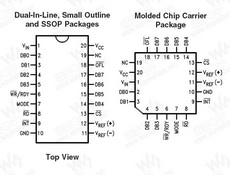
ADC0820 概述By using a half-flash conversion technique, the 8-bit ADC0820 CMOS A/D offers a 1.5 µs conversion time and dissipates only 75 mW of power. The half-flash technique consists of 32 comparators, a most significant 4-bit ADC and a least significant 4-bit ADC. The input to the ADC0820 is tracked and held by the input sampling circuitry eliminating the need for an external sample-and-hold for signals moving at less than 100 mV/µs. For ease of interface to microprocessors, the ADC0820 has been designed to appear as a memory location or I/O port without the need for external interfacing logic. |
|
||||||||||||||||||||||||||||
|---|---|---|---|---|---|---|---|---|---|---|---|---|---|---|---|---|---|---|---|---|---|---|---|---|---|---|---|---|---|
ADC0820 特性
|
|||||||||||||||||||||||||||||
