TLV1549
技术资料——
TLV1549 PDF技术资料
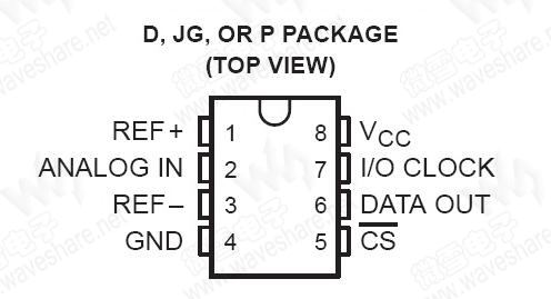
TLV1549 概述The TLV1549 are 10-bit, switched-capacitor, successive-approximation, analog-to-digital converters. The TLV1549 have two digital inputs and a 3-state output [chip select (CS\), input-output clock (I/O CLOCK), and data output (DATA OUT)] that provide a three-wire interface to the serial port of a host processor. The TLV1549C is characterized for operation from 0°C to 70°C. The TLV1549I is characterized for operation from -40°C to 85°C. The TLV1549M is characterized for operation over the full military temperature range of -55°C to 125°C. |
|
||||||||||||||||||||||||||||
|---|---|---|---|---|---|---|---|---|---|---|---|---|---|---|---|---|---|---|---|---|---|---|---|---|---|---|---|---|---|
TLV1549 特性
|
|||||||||||||||||||||||||||||