TLC549
技术资料——
TLC549 PDF技术资料
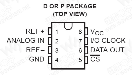
TLC549 概述The TLC549 are CMOS analog-to-digital converter (ADC) integrated circuits built around an 8-bit switched-capacitor successive-approximation ADC. The TLC549 are designed for serial interface with a microprocessor or peripheral through a 3-state data output and an analog input. The TLC549 use only the input/output clock (I/O CLOCK) input along with the chip select (CS\) input for data control. The maximum I/O CLOCK input frequency of the TLC549 is specified up to 1.1 MHz. The TLC549C are characterized for operation from 0°C to 70°C. The TLC549I are characterized for operation from -40°C to 85°C. |
|
||||||||||||||||||||||||||||
|---|---|---|---|---|---|---|---|---|---|---|---|---|---|---|---|---|---|---|---|---|---|---|---|---|---|---|---|---|---|
TLC549 特性
|
|||||||||||||||||||||||||||||