TLC272
技术资料——
TLC272 PDF技术资料
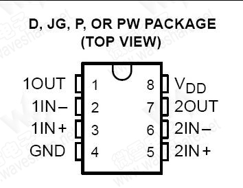
TLC272 概述The TLC272 precision dual operational amplifiers combine a wide range of input offset voltage grades with low offset voltage drift, high input impedance, low noise, and speeds approaching those of general-purpose BiFET devices. The TLC272 use Texas Instruments silicon-gate LinCMOS™ technology, which provides offset voltage stability far exceeding the stability available with conventional metal-gate processes. The C-suffix TLC272 are characterized for operation from 0°C to 70°C. The I-suffix TLC272 are characterized for operation from –40°C to 85°C. |
|
|||||||||||||||||||||||||||||||||||||
|---|---|---|---|---|---|---|---|---|---|---|---|---|---|---|---|---|---|---|---|---|---|---|---|---|---|---|---|---|---|---|---|---|---|---|---|---|---|---|
TLC272 特性
|
||||||||||||||||||||||||||||||||||||||