LPC2468
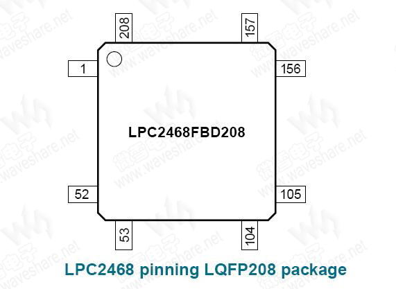
LPC2468 概述NXP Semiconductors designed the LPC2468 microcontroller around a 16-bit/32-bit ARM7TDMI-S CPU core with real-time debug interfaces that include both JTAG and embedded trace. The LPC2468 has 512 kB of on-chip high-speed flash memory. This flash memory includes a special 128-bit wide memory interface and accelerator architecture that enables the CPU to execute sequential instructions from flash memory at the maximum 72 MHz system clock rate. This feature is available only on the LPC2000 ARM microcontroller family of products. The LPC2468 can execute both 32-bit ARM and 16-bit Thumb instructions. Support for the two instruction sets means engineers can choose to optimize their application for either performance or code size at the sub-routine level. When the core executes instructions in Thumb state it can reduce code size by more than 30 pct with only a small loss in performance while executing instructions in ARM state maximizes core performance. The LPC2468 microcontroller is ideal for multipurpose communication applications. It incorporates a 10/100 Ethernet Media Access Controller (MAC), a USB full-speed Device/Host/OTG Controller with 4 kB of endpoint RAM, four UARTs, two Controller Area Network (CAN) channels, an SPI interface, two Synchronous Serial Ports (SSP), three I2C interfaces, and an I2S interface. Supporting this collection of serial communications interfaces are the following feature components; an on-chip 4 MHz internal precision oscillator, 98 kB of total RAM consisting of 64 kB of local SRAM, 16 kB SRAM for Ethernet, 16 kB SRAM for general purpose DMA, 2 kB of battery powered SRAM, and an External Memory Controller (EMC). These features make the LPC2468 optimally suited for communication gateways and protocol converters. Complementing the many serial communication controllers, versatile clocking capabilities, and memory features are various 32-bit timers, an improved 10-bit ADC, 10-bit DAC, two PWM units, four external interrupt pins, and up to 160 fast GPIO lines. The LPC2468 connects 64 of the GPIO pins to the hardware based Vector Interrupt Controller (VIC) that means these external inputs can generate edge-triggered interrupts. All of these features make the LPC2468 particularly suitable for industrial control and medical systems. |
|
|||||||||||||||||||||||||||||||||||||||||
|---|---|---|---|---|---|---|---|---|---|---|---|---|---|---|---|---|---|---|---|---|---|---|---|---|---|---|---|---|---|---|---|---|---|---|---|---|---|---|---|---|---|---|